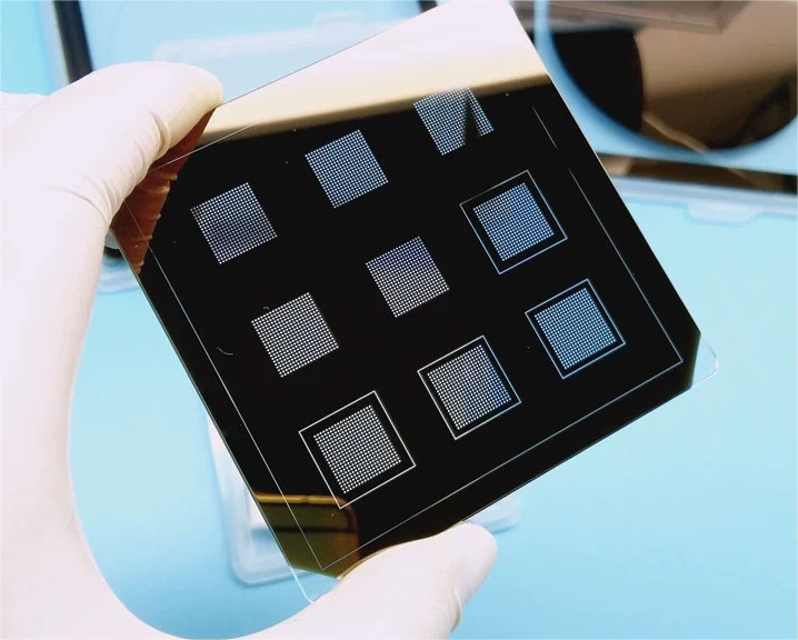
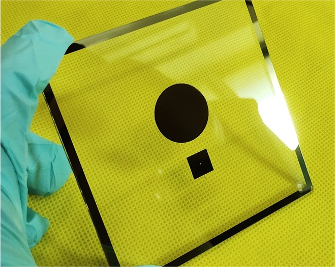
Laser direct writing lithography is to expose the resist material on the surface of the substrate with variable dose by using a laser beam with variable intensity, and then form the required relief outline on the surface of the resist layer after development.
 Product
 Service
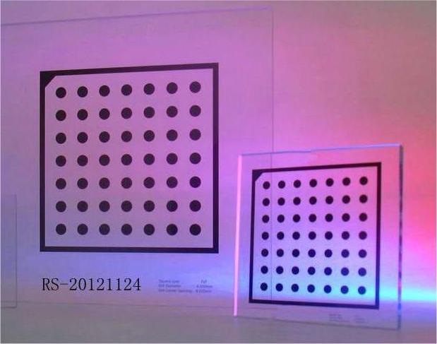
Laser direct writing
Product Details
parameter
Model
size
Download
The basic working principle of laser direct writing system is that the computer controls high-precision laser beam scanning, and the designed arbitrary pattern is directly exposed on the photoresist, thus the designed pattern is directly transferred to the mask. The laser direct writing system is mainly composed of He-Cd laser, acousto-optic modulator, projection lithography objective, CCD camera, display, illumination source, workbench, focusing device, He-Ne laser interferometer and control computer. The basic workflow of laser direct writing is: using computer to generate the designed micro-optical elements or VLSI mask structure data to be fabricated; The data is converted into direct writing system control data, and the computer controls the high-precision laser beam to directly scan and expose on the photoresist; The design pattern is transferred to the substrate through development and etching. Laser direct writing lithography technology is limited by laser wavelength, and its lithography accuracy is not as good as charged particle lithography technology such as electron beam and ion beam, which can not meet the needs of high-end semiconductor device manufacturing, but it is more suitable in photovoltaic field. At present, laser direct writing is more widely concerned and applied in the field of photovoltaic copper electroplating.
Usually, the seam of soda version is ≥ 2 um, and the CD accuracy is above ±0.2um; The seam of Shi Ying version is ≥ 1um, and the CD accuracy is above ±0.1um
3~14inch
3~14inch
No
Support Hotline
Learn about the latest product

Official WeChat
Links
丨


